Preparing transparencies (KiCad)
Home ► Electronics ► Circuit board fabrication ► Preparing transparencies (KiCad)
Prerequisites
Designing the circuit board
I use KiCad (http://kicad-pcb.org/) for the schematic and board design. It has the typical open-source quirks, and there are easier online options as well, but I prefer it nonetheless. I won't write up a full blown tutorial at this point, but here are some tips and tricks:
Select the right copper layer, especially for through-hole components
Seems like a no-brainer, but I've found myself working for an hour on a layout only to realise I should've put the tracks for the through-hole components on the back copper layer (B.Cu). You can change the layer a track is on, but it's a hassle to do for an entire board.
You can also correct this using the "Mirror" option when plotting, but it's best to be consistent.
Many symbols and footprints have already been created
If you find a symbol or footprint is missing from the standard library, Google for the part name for KiCad. There's plenty of GitHub repositories with components. I recommend placing them in the project folder and including it as a project-specific library.
Another good source of free symbols and footprints is https://www.snapeda.com/. You can create an account for free, and they offer free downloads in KiCad format for many components.
Plotting
I don't like to use KiCad's built-in Print option because it is limited to printing the layers in their position in the document. Instead I use the Plot option to output PDF files. These files can then be opened in Illustrator or the free Inkscape software (https://inkscape.org/) to position them on the page and compose multiple layers on a single sheet.
After printing the transparency it is a good idea to grab the components and match them against the print to see if the sizes match, because I've selected the wrong footprint in the design process more than once. I may have even etched and drilled a board before I figured out I accidentally selected the wide DIP package instead of a normal DIP. That was definitely a waste of time and material, but a very valuable lesson to always double-check along the way :-)
Orientation
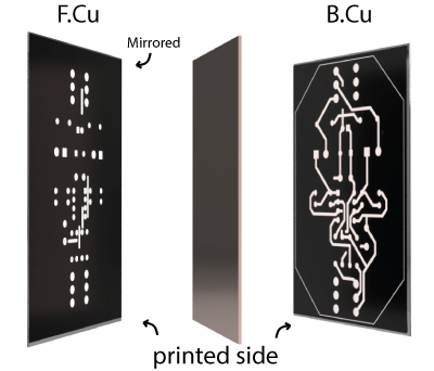
The use of the Mirrored plot option can be a bit confusing. The goal is to get the printed side on the film to minimize light bleed effects. Here's a visualization that may or may not help:
Back copper
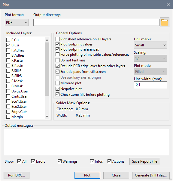
Select the B.Cu layer and optionally Edge.Cuts if you want the edges to show up as copper lines.
| Mirrored plot | Off | This will print the layer as though looking at it from the front, which means the printed side of the transparency can be directly on the film for the best results |
| Negative plot | On | Copper areas and tracks will come out as white and let the UV light through, curing the photosensitive film in those areas and protecting them from being etched |
| Drill marks | None / Small | Optional. If enabled, through-hole pads will have a small drill mark etched which makes it easier to guide the drill to the correct spot. |
Front copper
Select the F.Cu layer and optionally Edge.Cuts
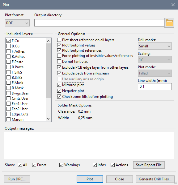
| Mirrored plot | On | This will print the layer as though looking at it from the back, which means the printed side of the transparency can be directly on the film for the best results |
| Negative plot | On | Copper areas and tracks will come out as white and let the UV light through, curing the photosensitive film in those areas and protecting them from being etched |
| Drill marks | None / Small | Optional. If enabled, through-hole pads will have a small drill mark etched which makes it easier to guide the drill to the correct spot. |
Back solder mask
Select the B.Mask layer
| Mirrored plot | Off | See Back copper |
| Negative plot | Off | Pads will come out as black and block the UV light from curing the paint |
Back solder mask
Select the F.Mask layer
| Mirrored plot | On | See Front copper |
| Negative plot | Off | Pads will come out as black and block the UV light from curing the paint |